
16 December 2021
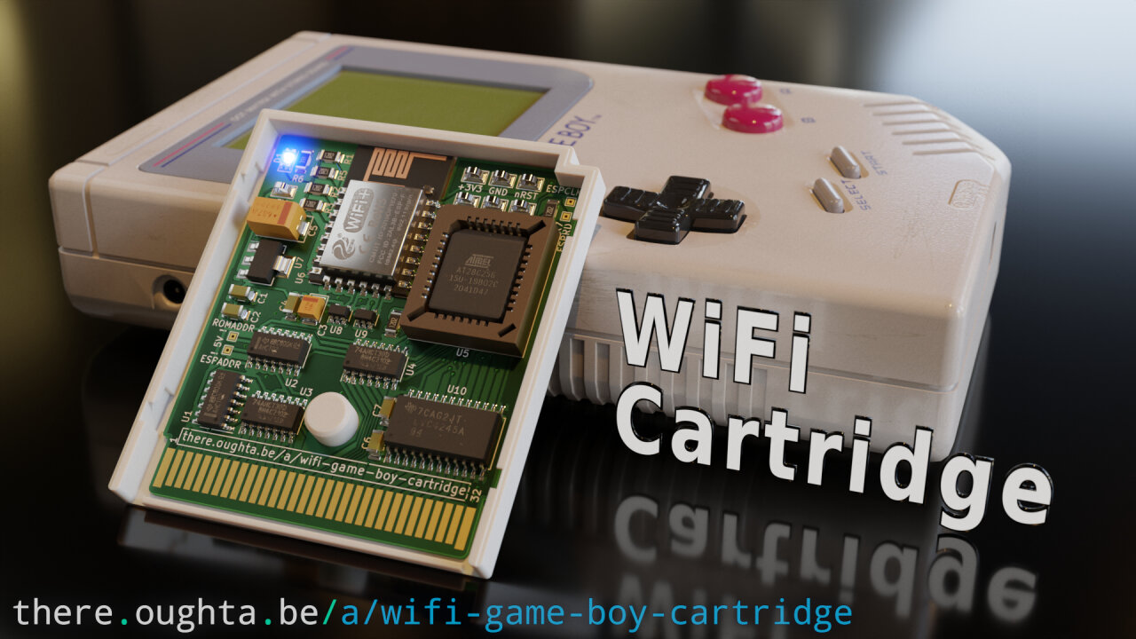
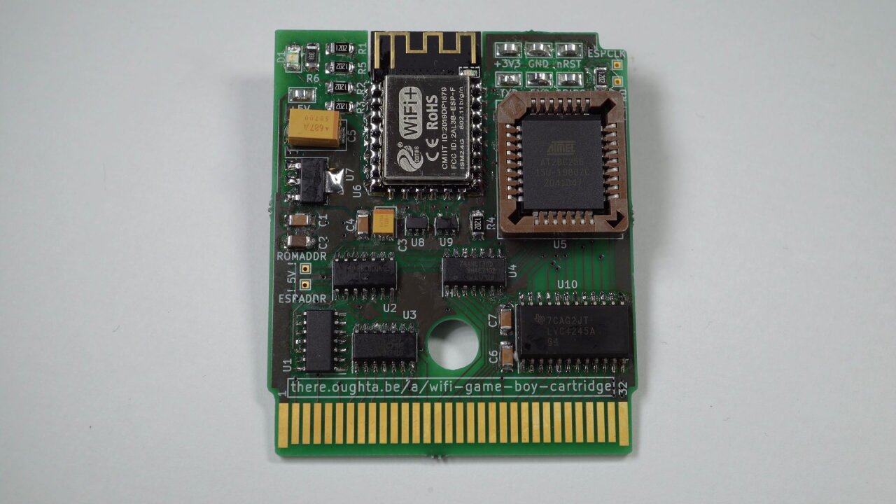
It took a while, but I finally managed to create my own Game Boy cartridge. With WiFi! At this point, it can only demo a simple telnet-style communication and access Wikipedia articles, but I am confident that I will showcase more in the future. For now, the interesting and surprisingly tricky part is how the thing works at all.
If you just want to see the cartridge in action or want to get into all the details, I highly recommend to watch the video first as it goes through the difficulties and their respective solutions. In contrast, this article here is less visual in its explanations and mostly documents the device in detail, so unless you are already familiar with the parallel memory interface of the Game Boy, you might want to start with the overview from the video.
Before you waste your time with this article, I should probably make clear what this cartridge can do and, maybe more importantly, what it cannot do. This is a basic 32kiB Game Boy cartridge with an ESP8266 microcontroller to add Wifi capabilities. With this, you can access data from the internet or your local network on your Game Boy or send data from it. Since the ESP8266 can do a lot of preprocessing for the Game Boy, a Twitter client is just as conceivable as a Reddit browser. If you implement one. This is not a generic browser, but you can relatively easily implement services on the ESP8266 and write simple code that is executed on the Game Boy as an interface.
At the time of writing this article, I have only implemented two demos: A simple communication demo that allows you to log onto the cartridge via telnet and send and receive text messages. And a Wikipedia client, which allows you to enter the title of an article1, then fetches the “extract” of that article and displays it.

This cartridge does not allow you to play your old games online or to access your ROM library via network. Playing old games online would only be possible if you were able to modify them massively, because they would have no idea what a network is, how to handle its delay and how network access even works on my cartridge design. Accessing the ROM library seems more realistic to me in principle, but since on my cartridge the Game Boy software is executed from a regular EEPROM which cannot be programmed by the micro-controller, this would require a redesign to either allow the ESP8266 to program the EEPROM with a binary from the network or to replace the memory entirely, which other projects did, but which has a few drawbacks as you will learn below.
Since I decided to add WiFi to a cartridge instead of adding WiFi to the link cable (for which two nice projects already exist 23), we should first discuss, how a Game Boy cartridge works and how we can communicate here. In contrast to the link cable that communicates at a leisurely 8 kHz rate, the Game Boy cartridges are not an interface to implement arbitrary communication, but a serious parallel memory bus, running at 1 MHz. Instead of comfortably sending some data to sync multiplayer games, it is the backbone of all Game Boy memory with a very specific protocol and a relentless clock.
If this sounds a bit over dramatic to you, I can tell you that the same bus is used by the Game Boy to access its internal RAM and VRAM. In fact, the cartridge will see (some of) those requests on the cartridge pins, too, so this interface really means business. If you want to know all the details, I would recommend the Game Boy CPU manual, but the short version is the following:
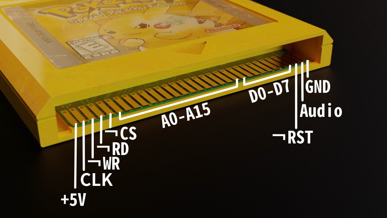
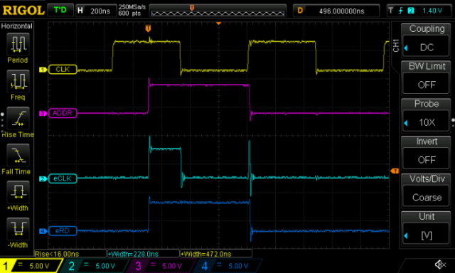
The cartridge connector offers 16 address pins and 8 data pins. On the address pins the Game Boy sets the memory address it wants to read or write and on the data pins it then reads or writes one byte of data. This access is controlled by a clock (CLK) pin, a read (RD) pin, a write (WR) pin and a chip select (CS) pin. RD and WR are used to declare if data should be read or written, while CLK gives a 1 MHz reference clock signal for read/write timing. The CLK is especially relevant as the RD and WR pins do not return to their off state between consecutive reads or writes, so it can be tricky to discern a sequence of reads if there is no clock.
The CS pin is actually not that relevant for our cartridge. Usually, a CS pin is used to enable or disable specific chips (therefore also known as chip enable or output enable) in order to switch between different chips on the same bus. However, in a simple4 Game Boy cartridge only the lower half of the memory is used by the ROM on the cartridge. 16 pins could address 64kiB of memory, but only 32kiB are on the ROM, while the remaining 32kiB are used to address internal memory (RAM, VRAM etc.) and registers (again, see the CPU manual for more details). Therefore, from the point of view of a basic cartridge, the highest address pin A15 acts as an inverted CS input as it is HIGH only for the upper 32kiB.
The cartridge connector also features a voltage supply through a +5V and a ground (GND) pin, which we use for the WiFi cartridge, and finally a reset (RST) and some kind of audio pin, which we do not need here.
Sounds like a straightforward interface, doesn’t it? My first idea of course was the modern universal maker solution: Hook up a modern micro controller to all those pins and solve the communication in software. We might need a few level shifters or bus transceivers and the sheer number of pins limits the suitable microcontrollers, but otherwise a modern 100 MHz micro-processor should have no trouble talking to a 4 MHz Game Boy CPU on a 1 MHz data bus, right? Well, it is in fact possible as an STM32 (168 MHz) cartridge by Emeryth and an RP2040 cartridge by u/LyneByLine (0xen) demonstrate. The latter even works with a Game Boy Color with twice the clock rate. However, the RP2040 had to be overclocked to 200 MHz, so just from the naive comparison of clock speeds, this seems to be at the limit of what can be done with this approach.
The problem is that the 1 MHz clock for the cartridge denotes memory cycles. One cycle equals one written or read byte. A CPU cycle may be more versatile, but a CPU cannot check the address pins, interpret their meanings, retrieve or even calculate the data that should be the response and set the output pins all in one cycle. As the projects demonstrate, it is able to do so, but this means that there is not much reserve to do anything else. The CPU can either keep an eye on the pins and really not do anything else or you could try to work with interrupts. But you only have 500ns to react on those interrupts and since you get read and write events all the time, even for internal memory access, the interrupt is firing all the time. The simple Arduino interrupts take a few µs to react, so those are out anyways. I am not sure how fast you can get with some assembly, but you would not free up much spare time for the CPU.
But we need some spare processing time. The CPU needs to tend to the WiFi connection, make requests for the Game Boy (like http requests to Wikipedia) and convert data for the Game Boy, because you certainly don’t want to parse Wikipedia’s JSON response on the Game Boy itself. Maybe newer multi-core micro-processors might help here and maybe one day davedarko will get his attempt at an ESP32-based WiFi cartridge to work, but right now I see these methods more as a proof of concept. So, I went for a more elegant solution (at least I think so) and got away with using just a dated ESP82665 (80 MHz) that was a leftover from another project.
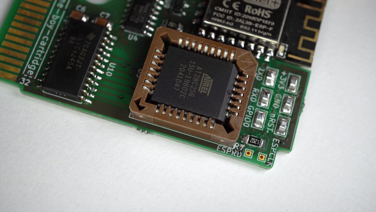
The idea is to cut down on the number of memory requests that the micro-controller has to handle as well as the number of pins it has to manage. So, first of all, instead of trying to replace the entire cartridge by a micro-processor, let’s use the component that is ideal to handle mundane memory requests: A good old 32kiB EEPROM. In fact, let’s start with mostly a basic 32kiB cartridge design, because after all, most of the memory requests will be static stuff like images or the byte code running on the Game Boy. Getting data from the network and therefore from the ESP is done less frequently.
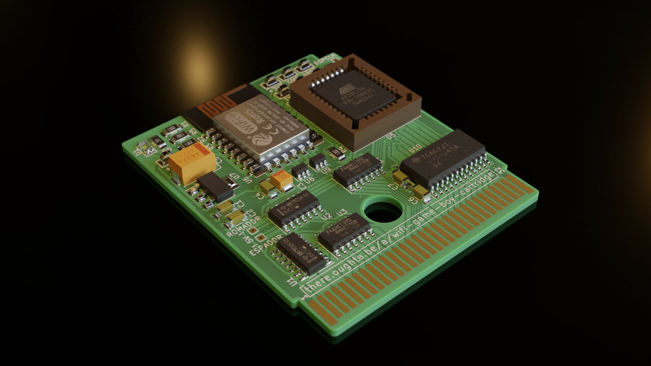
To actually get data from the ESP as well, I decided to map two bytes of the Game Boy’s memory space to the ESP8266: 0x7ffe and 0x7fff. If the Game Boy wants to read from the ESP, it accesses 0x7ffe to retrieve one byte after another, and if it wants to write a sequence of bytes to the ESP, it uses 0x7fff6. These two addresses have two advantages. They are at the very end of the regular 32kiB ROM space and only interfere with our program code if we were to use the entire 32kiB and they have a binary representation that makes it extremely easy to recognize them with a few logic gates. As 0x7ffe = 0b0111111111111110 and 0x7fff = 0b0111111111111111, all we need to do is invert the high bit A15 and put it through an AND gate (NAND in my design) together with all other pins down to A1. The result indicates whether the ESP is being addressed or not (ESPADDR) and the last bit A0 can be used to determine if it is being read from or written to. If we combine this last pin with ESPADDR, we get ESPRD, which is only high if the Game Boy tries to read from the ESP, which is also the only time at which the ESP ever should turn on the output on those pins that are connected to the data line D0 to D7.
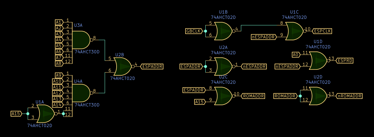
But most importantly, combining ESPADDR with the Game Boy clock through an AND gate (I actually used NOR logic instead) results in ESPCLK, which only ever goes high if the Game Boy wants to communicate with the ESP and which includes the falling flank of the original CLK signal, which is an important marker for the moment the Game Boy starts driving the data pins. This means that the ESP now only has to care about a single input which only changes if the ESP actually has to react and we only need ESPRD on a second pin to decide how to react to ESPCLK. The rest of the time, the ESP can do other stuff and mind its own business. The only imperfection here is that since the Game Boy changes the address slightly after the next clock rise, we get a little additional peak at the end of each ESPCLK, which we don’t need, but this can easily be filtered in software7.
These logic gates are also used to control the outputs of other components on the bus. The ESP with its 3.3V logic is connected to the Game Boy’s 5V data lines through a bi-directional bus transceiver and its output enable pin is directly controlled by ESPADDR to turn it off unless the ESP is in the loop. Similarly, a few more logic gates generate ROMADDR, which is only high if the address is in the range of 0x0000 to 0x7ffd to disable the EEPROM output in all other cases. Except for some possible temporal overlap of few nano seconds, this should eliminate most danger of bus contention, except for one: The ESP has to turn off its D0 to D7 outputs via software unless ESPRD is high. If it ever turns on the output while ESPRD is low and ESPADDR being high at the same time, it will work against the output of the bus transceiver and effectively cause a short circuit. So far, for me this only led to a brown out of Game Boy and ESP and of course it happened rather often during development, but I cannot guarantee that it might not eventually damage something.
Which leads us to the voltage supply for the cartridge. We have a mixed system with the ESP running on 3.3V logic and the EEPROM and logic gates using the same 5V as the Game Boy. So the 3.3V is converted from the Game Boy’s 5V by an NCP1117, which should have enough headroom. In fact, this is the same voltage regulator as used by the NodeMCU DevKit v1.0 and just like the NodeMCU I added a 100µF capacitor to stabilize the output along with the typical 100nF and 10µF pairs. Still, my first prototype had massive brown-out problems, so although I could not entirely rule out bus contention due to other design flaws in the first protoype, I added a 680µF on top. With this, the cartridge is quite stable - at least when the batteries are fresh. If they are just a bit depleted you start to see some memory corruption and even on full batteries you can hear static from the Game Boy speaker whenever the ESP8266 uses its WiFi module.
I suspect that the old linear voltage regulator of the Game Boy cannot handle the sudden current spikes of a WiFi module. The entire Game Boy uses a bit over 100mA at 5V. If we naively assume perfect efficiency of the power regulator, this translates to roughly 150mA at 3.3V. One should also note that this consumption should be relatively stable as the old hardware of the Game Boy does not switch rapidly between different power safe modes or change clock speeds like modern hardware does. In contrast, the ESP8266 can quickly change its power consumption to draw a current anywhere in the range from a few 10 µA to a whopping 200mA. In a normal use pattern, we can assume that it draws around 80mA (which would be fine for the Game Boy) and spikes up to 150mA when using the WiFi module, which is quite a blow for the Game Boy’s voltage regulator. I am not sure if just adding even bigger capacitors would really solve the problem, although the good thing about this situation is indeed that WiFi spikes seem to be short and the Game Boy seems to handle higher power consumption quite gracefully if it has time to adapt.
You can find the full schematics, PCB layout and gerber files in the github repository for this project.
With all the hardware in place, we can now set out to write our code. There are of course two pieces of software we need to write: The code that will be stored in the EEPROM to be run on the Game Boy and the software running on the ESP8266.
The Game Boy code is written using the Game Boy Development Kit gbdk-2020, which in case of these basic text based examples makes it extremely simple. Since gbdk-2020 implements stdio, we can simply throw a few putc, print and getc into a text editor to get the code we need. Until I try some more visual demos, the hard work is in the ESP code.
Because of habit and convenience, I wrote the ESP code in the Arduino IDE. There is nothing wrong with using simplified Arduino instructions as long as you know where to avoid them in favor of some optimization. The code basically connects to a WiFi access point with hardcoded credentials and monitors two character arrays as inbound and outbound buffer to the Game Boy. Depending on the actual demo, it will react to commands in the inbuffer and write results to the outbuffer, request webpages or convert data into text for the Game Boy.
The tricky part is how individual bytes are transmitted or received through the dedicated memory addresses. From the point of view of the ESP, it has to react to an interrupt monitoring ESPCLK and an interrupt on ESPRD8. But since it already takes a few microseconds before they even start executing their code, we have no chance to immediately react to something the Game Boy throws at us. Instead, we trigger on the falling edges (at that timing probably not really relevant) and use the interrupts to learn if the Game Boy just tried to read or write to prepare for the next event.
Since we run our own code on the Game Boy, we can teach it some patience and establish different communication patterns for reading and writing bytes from the ESP.
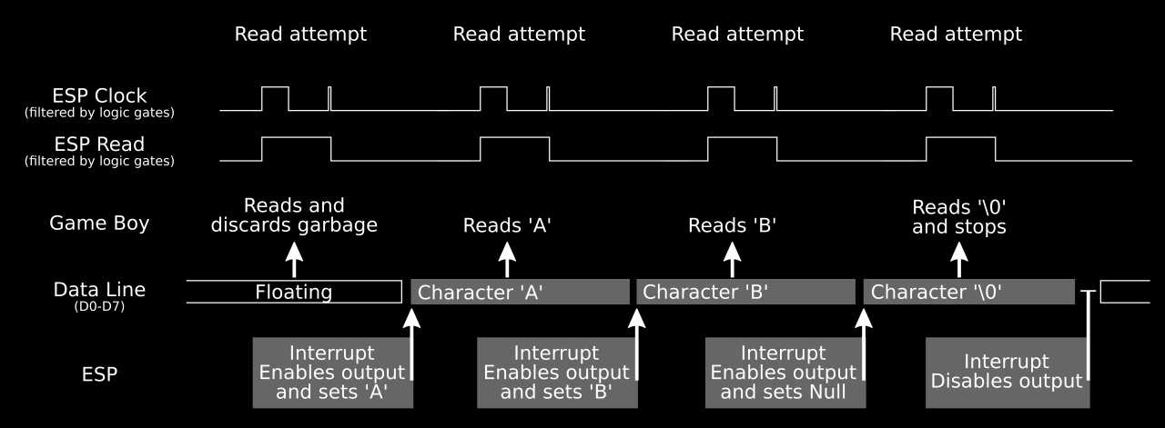
If the Game Boy wants to read from the ESP, it makes a first read attempt which will return garbage data, because the ESP did not even have enough time to turn on the GPIO output. But, the interrupt causes the ESP to turn the output on in time for the next read attempt and to set their outputs to the first byte to be transmitted. So, the Game Boy simply discards the garbage from the first read attempt and (if it is not retrying too fast, which is in our hands) can receive the first byte on the next read. This second read in turn triggers the interrupt on the ESP again, which can now set the outputs to the second byte. Therefore, after discarding the very first read attempt, the Game Boy can just sequentially read more bytes without wasting any more read attempts. It just needs to make sure to be slow enough. In order to stop when there is no data left to read, the ESP sends 0x00 as the last byte, which is perfect for transmitting null terminated strings. After the interrupt was triggered while 0x00 is already set at the output, the ESP turns off its output and, conversely, the Game Boys stops reading after encountering 0x00.
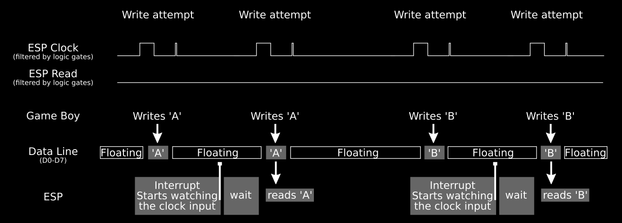
Sending data from the Game Boy to the ESP8266 is actually a bit trickier. The problem is that the Game Boy only drives the data bus for 500ns and we cannot change that. When reading from the ESP, the ESP can just turn on its outputs indefinitely and wait until the Game Boy has picked up the data, but when the Game Boy writes to the ESP, the ESP gets a 500ns window to catch that byte and that’s it.
We can, however, send the same value multiple times. It still requires good timing on behalf of the ESP, because this only means that there will be another 500ns window after a gap, but this allows us again to use the first write as a trigger. So, in order to write a byte to the ESP, the Game Boy sets address 0x7fff to its value, which triggers the interrupt on the ESP way too late. This time, the Game Boy stays in the interrupt function for a few microseconds and just starts reading ESPCLK in a loop, waiting for it to rise, indicating another write. The Game Boy then simply writes the same value again to 0x7fff, but this time, the Game Boy does not have to wait for an interrupt. It notices the rising ESPCLK within a few of its cycles, waits further for it to fall again (which happens when the Game Boy starts driving the data bus for 500ns, see CPU manual) and then reads the byte within the 500ns window without any trouble. Only downside is that unless we want the CPU to permanently watch ESPCLK, it now again has to be triggered by an interrupt first and therefore, the Game Boy needs to send each byte twice with a short pause between writes.
However, there is not that much data to be sent from the Game Boy itself - at least I cannot think of much to send from the Game Boy to the ESP except for user input and some requests initiated by user actions. So, it seems fitting that writing to the ESP is a bit slower than receiving from it.
Oh, and there is one little confusing detail, which best fits into this section: For some reason, I have to turn on the internal pull-up resistors for the GPIO-pins of the ESP8266 that are connected to the bus transceiver for D0 to D7. If I don’t, some of these pins (those that do not have an external pull-up anyways) would not go low when the ESP sends data. I assume that it has something to do with the way I enable the output through the ESP’s GPES register. Maybe I end up in some kind of Open Drain configuration, which of course would require the internal pull-ups? If someone spots the reason, I would love to learn about it.
Ok, as the title of this section suggests, I am sharing all the hardware schematics and the source code, so you can build your own version. However, before you scream “Hell, yes!” and pull out your soldering iron, you should carefully look at the following warnings, required tools and recommended skills.
| Quantity | Part Number | Manufacturer | Description |
|---|---|---|---|
| 1 | 2491 | Adafruit | 802.11 ESP8266 SMT Module - ESP-12F |
| 1 | 69802-432LF | FCI / Amphenol | Component Sockets 32P PLCC SOCKET |
| 1 | AT28C256-15JU | Atmel | EEPROM 256K 32K x 8 150 ns 4.5V-5.5V |
| 2 | 74AHCT30D-Q100J | Nexperia | Logic Gates 8-input NAND gate |
| 2 | SN74AHCT02D | Texas Instruments | Logic Gates Quad 2-Input |
| 1 | SN74LVC4245ADWRG4 | Texas Instruments | Octal Bus Transceiver 3.3V To 5V Shifter |
| 2 | SN74LV1T34DBVRG4 | Texas Instruments | Voltage Levels Single Power Supply BUFFER Logic Level Shifter (no enable) 5-SOT-23 -40 to 125 |
| 6 | RC1206FR-0712KL | YAGEO | SMD Thick Film Resistors - SMD 12 kOhms 250 mW 1206 1% |
| 1 | CRGCQ1206J330R | TE Connectivity | SMD Thick Film Resistors - SMD CRGCQ 1206 330R 5% SMD Resistor |
| 1 | C1206C106K8PAC | KEMET | SMD/SMT Multilayer Ceramic Capacitors MLCC - SMD/SMT 10V 10uF X5R 1206 10% |
| 4 | C1206C104M5RACTU | KEMET | SMD/SMT Multilayer Ceramic Capacitors MLCC - SMD/SMT 50V 0.1uF X7R 1206 20% |
| 1 | TAJE687M010RNJV | Kyocera AVX | Tantalum Capacitors - Solid SMD 10V 680uF 20% 2917 ESR= 400 mOhm |
| 1 | TAJB107M010RNJ | Kyocera AVX | Tantalum Capacitors - Solid SMD 10V 100uF 1210 ESR=1.4Ohms 20% |
| 1 | 156120BS75000 | Wurth Elektronik | SMD Standard LEDs - SMD WL-SMRW RvsMnt Mono Rect 1206 Blue |
| 1 | NCP1117IST33T3G | onsemi | LDO Voltage Regulators ANA 1.0A 3.3V LDO REG |
| 7 | 5015 | Keystone Electronics | PCB MINI SMT TEST POINT |
After soldering your PCB, it is time to build the software. You can find all the code on github in the folders “esp8266” and “gb” with (you guessed it) the code for the ESP8266 and the Game Boy respectively. Note that each folder contains subfolders with matching names for each demo. You have to make sure that you always use the matching code for the ESP and the Game Boy. Do not, for example, mix the serial demo with the wiki demo. Hopefully, I will add a few more demos here in the future.
In order to build the software for the Game Boy, you need to download a gbdk-2020 release and unzip it such that the resulting gbdk folder is next to the gb folder. After that you should be able to just go into the “gb” directory and type “make” to build all demos (if you have trouble on operating systems without a proper command line (i.e. Windows), look into the gbdk-2020 documentation for instructions on how to build projects there). As a result, you should find a .gb file in each demo folder, which you need to write to your EEPROM with your programmer. That’s it. Just pop the EEPROM into the PLCC32 socket on the cartridge and the Game Boy part should be ready to go.
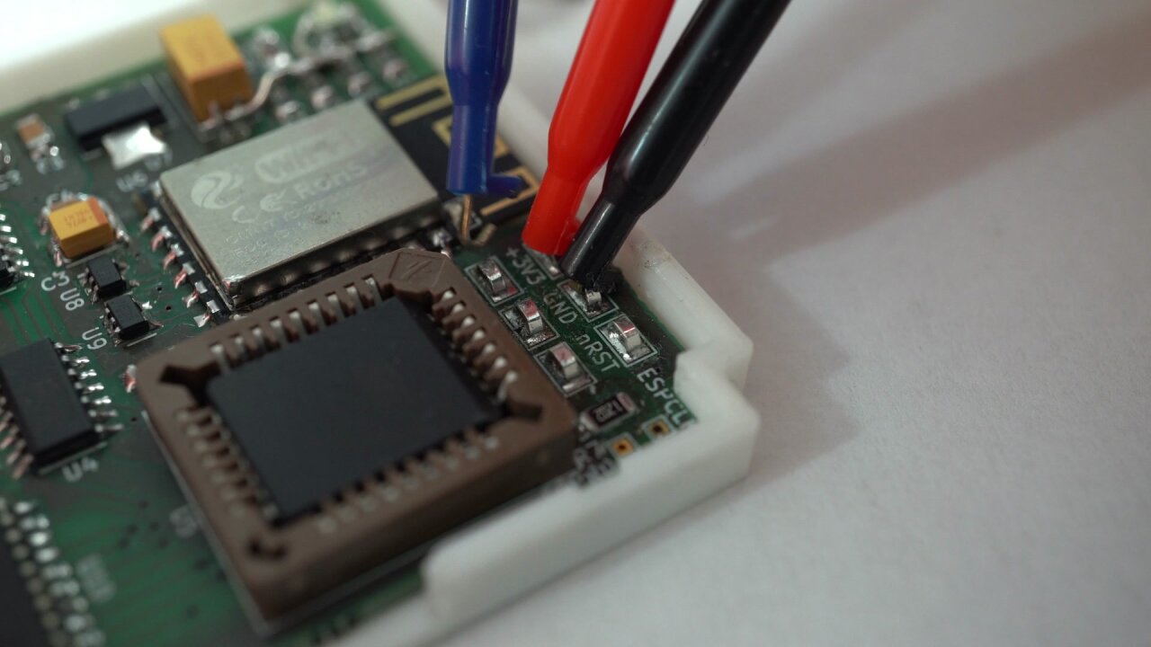
In the “esp8266” folder you will find Arduino projects, that you can simply open in your Arduino IDE. Make sure to edit the “secrets.h” file to set your WiFi credentials10. You can simply compile and upload the code from the Arduino IDE as you would to any other ESP8266 (make sure to set up and select the right board), but you need to figure out the correct wiring first. There are plenty tutorials and examples on the web on what you can use to program an ESP-12F and how to connect a USB to serial adapter here. If you used the Keystone test points from the parts list above, you can use hook connectors to secure the cables during programming. For most setups, you just need to connect 3V3, GND, RXD and TXD.
Also, take a look at the schematics and you will find that the PCB has all the resistors in place to boot the ESP8266 into execution mode by default, so you will need to connect GPIO0 to GND while resetting the ESP by shortly connecting nRST to GND (the equivalent to holding BOOT while pressing EN on a development board) to get it into programming mode. Make sure that your Game Boy is turned off while programming the ESP as there is no diode to prevent current from flowing back into either voltage source.
At this point, you can probably push the PCB directly into the Game Boy. However, I recommend printing at least the lower half of the cartridge shell as it makes it easier to handle it. Just pick the STL files from github or from thingiverse, slice them at the finest setting for your printer (it’s not a large print anyway) without supports and print them. Note, that my PCB has a thickness of 1.6mm and I modified the cartridge to have rather thin walls to account for this rather thick PCB as well as for the height of the EEPROM socket. I doubt that this PCB will fit into any normal Game Boy cartridge.
Now you have your very own WiFi Game Boy cartridge and are obliged to let me know what you do with it :)
Despite the fact that the resulting cartridge is nowhere near anything that could be used in production I am really happy about the result. In the end, I just wanted to proof to myself that I understand the old hardware well enough to extend it with modern tools. In terms of usefulness, I do not see much that could be done with this that could not be done with better and newer tools than a Game Boy. Granted, they have been so widespread that they are available cheaply despite their nostalgia value, but while they are very sturdy and reliable, the screen is so bad from our modern point of view that it becomes very annoying to use a Game Boy.
With much cheaper and better alternatives for handheld devices today, I only see a nostalgia value here. Maybe someone wants to open a retro-themed restaurant where guests can order from WiFi-enabled original Game Boys? Well, nostalgia is definitely worth something. I did not have that much fun with a project in a while and picking up the old Game Boy for a hundredth time during development still brought a smile to my face.
I hope that I can do a follow up with some more complex and maybe visual demos than just pushing text through the network.
In case you find this onscreen keyboard impressive: This is not my work, but the default keyboard offered by the Game Boy Development Kit gbdk-2020. This is part of their stdio implementation that I use in this demo. ↩
A project that demonstrates link cable WiFi with a custom game by Andy West. ↩
Playing Tetris via a WiFi link cable with more than two players ↩
There are larger Game Boy cartridges, which use a so-called Memory Bank Controller (MBC), that allows mapping different areas of a larger memory to this 32kiB section. ↩
To be precise, I am using an ESP-12F module. ↩
This could also be determined using the RD or WR pin, but when I designed the solution I wanted to avoid the WR pin as it is set rather late in a cycle (see CPU manual). However, now that it is working, I think that the RD pin alone could have been used in combination with only one address for the ESP. But nobody cares about wasting a single byte, so I do not redesign the entire PCB just to be a bit (well, a byte) more efficient. ↩
I am not even entirely sure if this peak even triggers the interrupt, because it is too slow. Yes, if the interrupt is already running, it can be triggered again, but at this point we have not even entered the interrupt function of the previous trigger. ↩
As the interrupt is too slow to immediately check ESPRD after a rising ESPCLK triggered it, we need to discern them through individual interrupts. ↩
Since this is specific to the order from Aisler, I took most images here before fixing the problem. But if you look closely at shots of the working PCB, for example in the video when putting the cartridge into the Game Boy, you can see some silver wire in the top left corner near the LED that I used to make the 3.3V connections as well as a nearly invisible one at the 100µF capacitor. ↩
…or develop a Game Boy interface to select a WiFi network for all of us :) ↩